Assembling Logic
Using functional parts such as flip-flops, we can assemble frequency dividing circuits which can be use to time and control actuation signals in a structure like the walking motor. This shows a design interface (top) for hierarchical design of discrete lattice assembly. (Middle) conductive elements highlighted to show underlying wiring between logical elements and actuators. Dual electronic/mechanical simulation of assembly results in 2 degree of freedom motion of end effector (bottom).

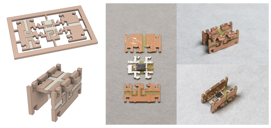
We have begun physically fabricating parts towards the goal of assembling logical structures and circuits that could be used to control a robot. This part contains a flip-flop IC and the required routing to interface with our assembly architecture. As a strut in this architecture, this part connects two nodes together, providing inputs for D, CLK, GND, and VCC and outputs for Q, GND, and VCC.
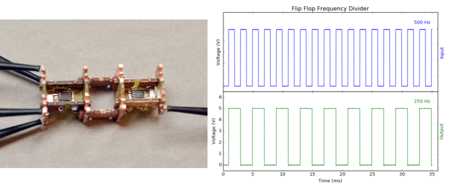
Here we measure and validate the performance of a single flip-flop part acting as a frequency divider. We provide an input square wave at 500Hz and measure an output square wave with 250Hz, as expected.
In decomposing functionality further, we can parts with a single logic element can serve as the basis for the assembly of structures that can compute. Pictured here, is a design of a logic block which embeds the smallest commercially packaged logic IC’s (SOT1226) onto a strut which can be assembled in our lattice architecture.

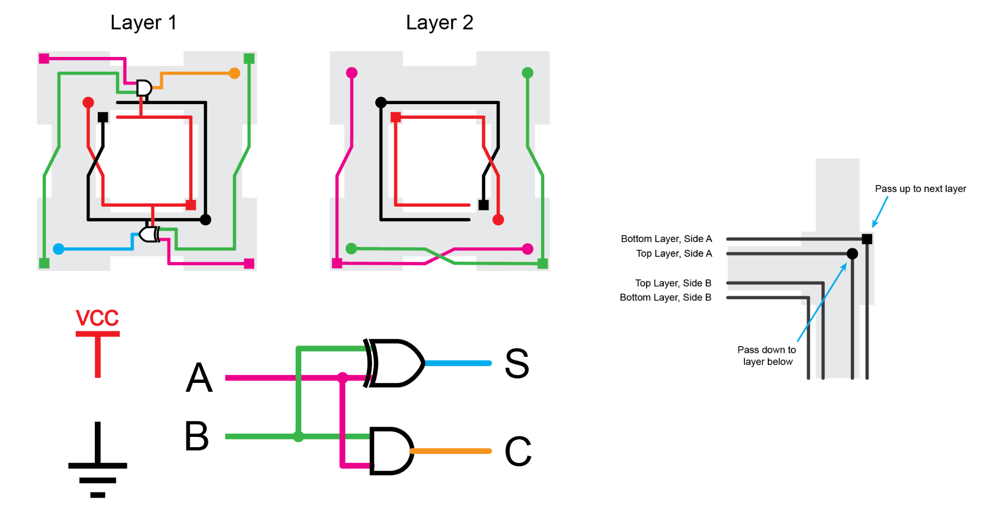
With these logic-level building blocks we can assemble computational components like a half-adder. In this case, an XOR block and an AND block are wired to produce a SUM and a CARRY output from A and B inputs.
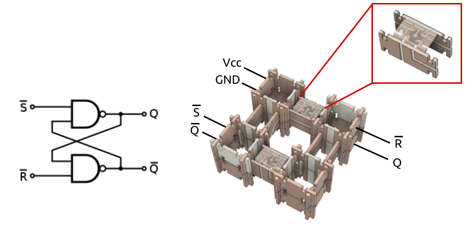
An SR flip flop can be made from two NAND gates. We can therefore assemble an SR flip flop with two NAND logic blocks and a few additional parts to route the required traces. We have found three node part-types (conductive, insulating, and split-conductive) as well as four strut part-types (conductive, insulating, split-conductive, and crossover) to be necessary for routing most schematics.
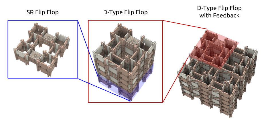
A D-type flip flop augments an SR flip flop with two additional NAND gates such that the state can be latched and unlatched with a clock pulse. We can assemble a D-type flip flop with three additional layers to house the two extra NAND gates and an inverter. Furthermore, we can add routing to connect Q-NOT to the D-input to configure this flip flop to serve as a frequency divider with feedback.
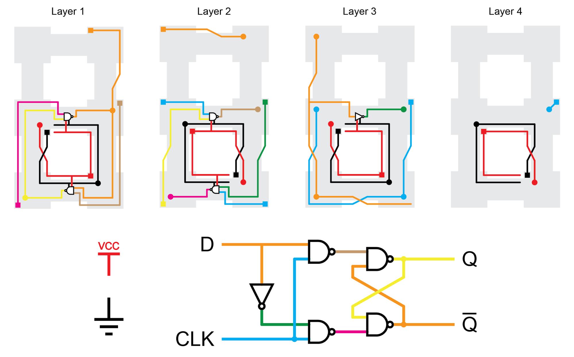
Here, we show the routing diagram to reproduce the desired circuit (above) out of our assembly architecture. Power and ground are routed on inner loops of the structure such that they are accessible to all components in the system and so that the signal wires are accessible from the perimeter. Most of the routing is accomplished in a 2x2x3 grid of our lattice with the exception of the feedback loop connecting Q-NOT to D (required for serving as a frequency divider).
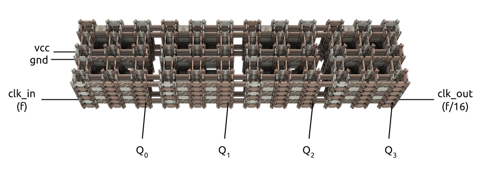
With the D-type flip flop structures as building blocks, we can then assemble higher-level assemblies like a ripple counter or frequency divider. This structure takes a clock pulse in and counts in binary on the Q outputs and provides an output square wave at one-sixteenth the frequency.
